Interview Questions on Clock Domain Crossing CDC and synchronizers Part 1
clock domain crossing interview questions
A digital circuit with flip flops will always have clocks associated to it and circuits with only one clock domain are normally restricted to elementary school courses. The modern SoCs, with so many dedicated data processing islands usually need to transfer data between these multiple clock domains (islands). When data needs to be transferred between two different clock domains, it will appear to be asynchronous to the new clock domain.
The above mechanism does have one drawback in terms of bandwidth usage of the interface. For handshaking mechanism, the data bus cannot be updated while receiving the ack signal. For applications where this is a bottleneck, this can be solved by using Dual Clock Asynchronous FIFO. Correctly designed FIFOs can increase bandwidth across the interface while still maintaining reliable communication across channels.
This Clock Domain Crossing (CDC) technique requires a dual port SRAM, a source control block which controls the write pointer (address where the data should be written in SRAM), a destination control block which generates the read pointer (address where the data should be read in SRAM) and binary to gray encoder blocks along with 2-FF synchronizer circuits. The pointers are managed as circular buffer by respective control blocks. However, to know when to write (FIFO not being FULL) and when to read (FIFO not being empty), the source and destination control blocks need to have a view of read and write pointers respectively. Transferring of the pointers to another clock domain is not straight forward. Since pointer is a multibit signal so using a 2-FF synchronizer directly is not an option. For this reason, both pointers are passed through a Binary to Gray Encoding block. This makes sure that values when transferred, only one bit of the vector gets updated from one clock to another clock and thus eliminates the problem of synchronizing multibit bus on a clock edge. An example of 4-bit Gray Encoder is shown below
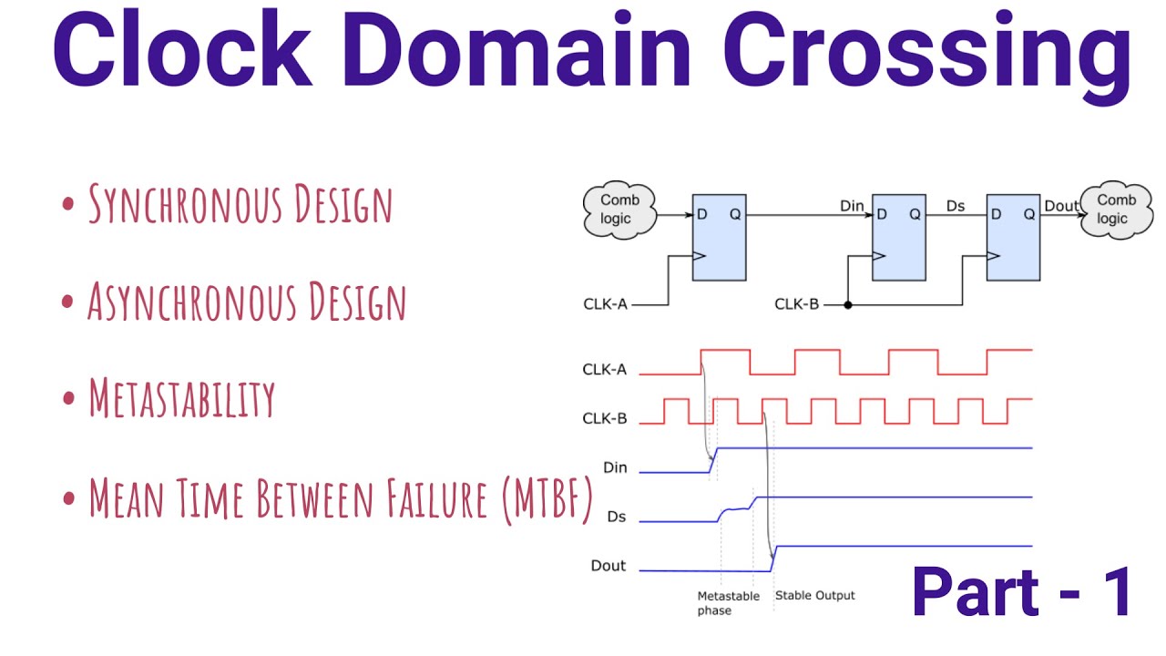
For proper operation of the flip flops, the inputs and clocks must satisfy the setup and hold requirements of the FFs. In figure 2 above, the signal A is asynchronous to destination clock domain, since there is no relation between clk_A and clk_B. Once an asynchronous signal is encountered into a clock domain, the setup and hold timings constraints are very unlikely to be met, and thus the FF can enter a metastable state. In picture below the output A of the FF-A changes very close to the pos-edge of the clk_B and thus violates the setup of the FF-B. The output of FF-B will go into metastable state and thus cannot settle to either 1 or 0. This can lead the downstream FFs in the clk_B domain sample wrong value or worse go into metastable state as well.
In handshake technique, the source domain sends the “request” signal to destination domain which uses a 2-FF synchronizer. Once the destination domain receives the request, it sends an “ack” signal to the source domain which uses 2-FF synchronizer to synchronize it. The ack signal indicates to the source that destination has received the value and source can update its value. There are many implementation versions of the handshake mechanism, but the principle remains the same – synchronizing the request and ack signals. The same technique can be applied to do a data bus transfer from source clock domain to destination clock domain. The request will indicate a new value on the bus where as ack will indicate that data bus can be updated.